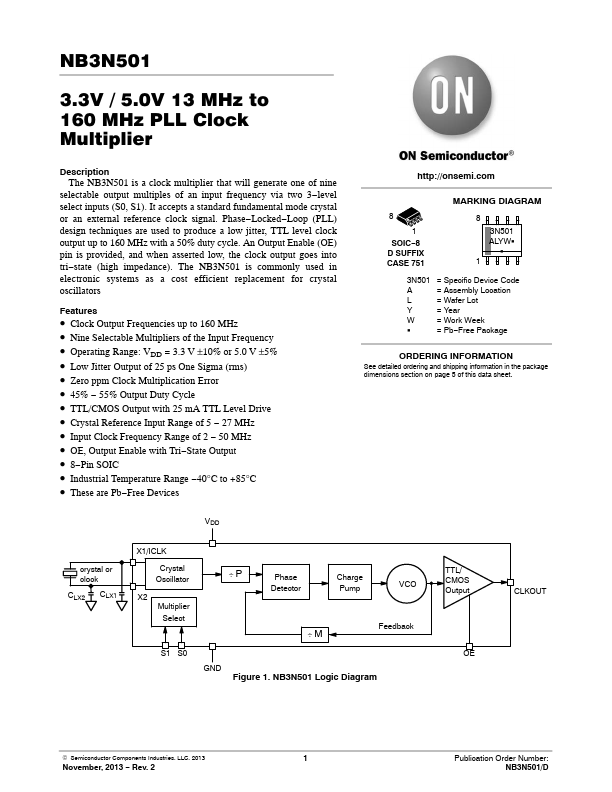
Datasheet4U Logo Datasheet4U.com

NB3N501 - 3.3V / 5.0V 13 MHz to 160 MHz PLL Clock Multiplier

General Description

The NB3N501 is a clock multiplier that will generate one of nine selectable output multiples of an input frequency via two 3

level select inputs (S0, S1).

It accepts a standard fundamental mode crystal or an external reference clock signal.

Locked Loop (PLL) design tech

Key Features

  • Clock Output Frequencies up to 160 MHz.
  • Nine Selectable Multipliers of the Input Frequency.
  • Operating Range: VDD = 3.3 V ±10% or 5.0 V ±5%.
  • Low Jitter Output of 25 ps One Sigma (rms).
  • Zero ppm Clock Multiplication Error.
  • 45%.
  • 55% Output Duty Cycle.
  • TTL/CMOS Output with 25 mA TTL Le.

📥 Download Datasheet

Datasheet Details

Part number NB3N501
Manufacturer onsemi
File Size 102.32 KB
Description 3.3V / 5.0V 13 MHz to 160 MHz PLL Clock Multiplier
Datasheet download datasheet NB3N501 Datasheet

Full PDF Text Transcription (Reference)

The following content is an automatically extracted verbatim text from the original manufacturer datasheet and is provided for reference purposes only.

View original datasheet text
NB3N501 3.3V / 5.0V 13 MHz to 160 MHz PLL Clock Multiplier Description The NB3N501 is a clock multiplier that will generate one of nine selectable output multiples of an input frequency via two 3−level select inputs (S0, S1). It accepts a standard fundamental mode crystal or an external reference clock signal. Phase−Locked−Loop (PLL) design techniques are used to produce a low jitter, TTL level clock output up to 160 MHz with a 50% duty cycle. An Output Enable (OE) pin is provided, and when asserted low, the clock output goes into tri−state (high impedance).